Installing an RP2040 Modchip on the Nintendo Switch OLED — The Kamikaze Method
Introduction
The Switch OLED requires a modchip to run custom firmware because it cannot be exploited via RCM like unpatched Switch V1 consoles. A modchip works by performing CPU voltage glitching to bypass bootROM firmware verification, then launching a payload.bin file from your microSD card.
- DAT0 Adapter method — the recommended approach for most installers, using an interposer board between the eMMC and motherboard.
- Kamikaze method — covered in this guide, which involves grinding down through the third layer of the motherboard to expose the DAT0 trace directly.
The Kamikaze method was developed as a collaboration between Stashboy and DefenderOfHyrule and is considered the more permanent solution, but it is unforgiving — grinding even a fraction of a millimeter too deep can sever the trace and brick the console.
The only community-supported RP2040 modchip is Picofly (pre-made variants and DIY builds using an RP2040-Tiny dev board).
Tools & Materials Required
Standard Installation Tools
Soldering Iron
Temperature-controlled, small tip, capable of reaching 350°C consistently.
Quality Flux
Essential for clean solder flow on fine pads.
34–38 AWG Wire
Single-core Kynar wire recommended.
Screwdriver Bits
+00 Phillips and Y1.5 tri-point for the OLED chassis.
Isopropyl Alcohol
95–99% IPA for cleaning thermal paste and the grind area.
Thermal Paste
Non-conductive. Reapply to the SoC die during reassembly.
Kapton Tape
Protects solder joints from thermal paste corrosion.
Double-Sided Tape
For securing the modchip to the IHS.
Microscope
Strongly recommended — Kamikaze is not possible without one.
Fume Extractor
For your own health and safety during long sessions.
Kamikaze-Specific Tools
Grinding Pen
MaAnt D2 or equivalent with a 0.2mm tip. Non-negotiable.
Fine Solder
0.8mm diameter or smaller, rosin core.
TS-J02 Tip
Fine iron tip well suited for trace-level soldering.
UV Solder Mask
Required to secure the wire and protect the exposed trace.
UV Light
For curing the solder mask, 1–3 minute cure time.
Enameled Magnet Wire
32–36 AWG for the trace connection.
Multimeter
Required for diode-mode verification of the exposed trace.
Low-Melt Solder Paste
Optional — easier than wire solder for tiny trace work.
Tweezers
For guiding the magnet wire onto the solder ball.
Disassemble the Switch OLED
Full disassembly photos and screw diagrams are available on iFixit. The key steps relevant to this installation:
- Unscrew the backplate.
- Remove the metal shield/cover — be careful with the antennas routed across it.
- Disconnect the battery connector at the bottom right of the motherboard.
- Remove the Gamecard / SD card reader board.
- Remove the heatpipe and heatsink assembly.
- Remove the IHS (Internal Heat Spreader) to expose the bare SoC die and RAM chips.
- Clean all thermal paste off the SoC die and from between the capacitors on the SoC using IPA. The red-ish thermal goop between the heatpipe and metal shield can be left alone.
- Remove the fan and unplug the fan ribbon, joycon rail ribbons, screen ribbon, and speaker connectors.
- Unscrew and remove the bottom bar of the shell.
- Remove the motherboard from the casing.
Note
Signal Points & Diode Values
| Label | Signal | GPIO (RP2040-Tiny) | Notes |
|---|---|---|---|
| C | DAT0 | Pin 29 | Exposed via Kamikaze grind, 1mm from A point |
| A | CMD | Pin 28 | Bottom end of the CMD resistor |
| D | CLK | Pin 27 | Requires solder mask scraping on OLED |
| B | RST | Pin 26 | Alternative via above the left speaker connector (recommended) |
| — | 3.3V | 3.3V pin | 3.3V capacitors near top-middle of motherboard front |
| — | GND | GND pin | Ground pad on middle-right side of motherboard |
| Point | +Probe to GND | −Probe to GND |
|---|---|---|
| SP1 | ~0.420 | ~0.520 |
| SP2 | ~0.25 | ~0.20 |
| A (CMD) | ~0.470 | ~0.875 |
| B (RST) | ~0.405 | OL |
| C (DAT0) | ~0.435 | ~0.450–0.850 |
| D (CLK) | ~0.440 | ~0.880 |
| 3.3V | ~0.445 | ~0.850 |
Note
Cut the SoC Frame
Surrounding the SoC die is a metal bracket — commonly called the SoC frame (sometimes the heat shield bracket). It sits between the motherboard and the IHS, helping retain the heat spreader. You need to make two cuts in this frame before any further work:
- A notch over the D (CLK) point so the pad becomes accessible for soldering later.
- A notch on the opposite side of the SoC so the SoC ribbon cable can exit cleanly when reassembled.
- Identify the section of the SoC frame covering the D (CLK) point — the strip of metal between the SoC and the CLK area.
- Using a sharp cutter, dremel with a fine bit, or fine flush cutters, carefully remove just enough of the frame to expose the CLK pad. Do not remove more than needed.
- Identify where the SoC ribbon cable will exit (the opposite side of the SoC, between the SoC and RAM). Cut a small notch in the frame at that location.
- Clean all metal shavings off the board with a brush, compressed air, and IPA.
Grind to Expose the DAT0 Trace
This is the heart of the Kamikaze method. You will grind through three layers of the motherboard — two copper layers and two interposer (fiberglass) layers — to expose the DAT0 trace directly. The trace is exactly 1mm away from the A (CMD) point.
- Identify the grind area, 1mm away from the A (CMD) point. Outline the zone you will stay within mentally before starting.
- Apply flux or IPA to the grind area to suppress debris scatter.
- Begin grinding an outline you will stay within throughout the process.
- Grind through the entire first copper layer evenly. Keep applying flux or IPA to keep the area wet.
- Continue through the first brown interposer layer (silicon/fiberglass). These layers sit between every copper layer in the motherboard.
- Once through the first interposer, you've reached the second copper layer. This is where it gets very risky. Grind evenly and slowly.
- Continue through the second interposer layer. The DAT0 trace lies directly underneath.
- Apply flux or IPA to make traces visible. You will see several traces — look for the one with a circular tip pointing toward CMD/A. That's DAT0.
- Grind only the circular part of the DAT0 trace to expose it. Grinding any deeper severs the trace and bricks the console.
Verify the Exposed Trace
- Clean the grind area completely. It will look very dry after cleaning — this is normal.
- Give the system a test boot to confirm you haven't bricked it.
- Verify with a multimeter in diode mode: place the negative lead on the exposed trace and the positive lead on ground. You should read between
~0.450and~0.850.
Scratch the D (CLK) Point
- Scrape away the solder mask on top of the D point using a thin, sharp metal tool until the copper pad underneath is exposed.
- Pre-tin the exposed copper so it's ready to take the ribbon pad later.
Mask, Solder, and Wire the DAT0 Trace
- Apply UV solder mask to the grind cavity, but leave the DAT0 trace itself uncovered.
- Cure the mask with UV light for 1 to 3 minutes (depending on lamp strength).
- Apply a small solder ball to the exposed trace. Alternatively, use low-melt solder paste and a hot air station to form the ball.
- Cut a piece of enameled / magnet wire (32–36 AWG) and pre-tin one end.
- Apply flux to the solder ball.
- Use tweezers to guide the wire onto the ball. Use your iron at 350–360°C — you're three layers down, so it takes real heat to reflow the joint.
- If the wire connection is weak, dab some UV solder mask onto the wire to hold it in position, then apply a touch more solder to strengthen the joint. (Low-melt solder + hot air is the alternative.)
- Once secure, cover the entire grind area with UV solder mask and cure for 1 to 3 minutes.
Place & Solder the Top Ribbon (3.3V, C, A, D, Anchors)
- If desired, trim the MvOLv6 ribbon cable to length so it lines up cleanly with the C, A, D, and 3.3V points without excess slack.
- Line the ribbon up over the board so its pads sit directly on 3.3V, C, A, and D, with the anchor pads landing on bare board.
- Tack one anchor or corner first to hold alignment, then verify all four signal pads are still seated correctly under magnification.
- Solder all points in one workflow: 3.3V, C (DAT0), A (CMD), D (CLK), and the ribbon anchors. The D pad was already scratched and tinned in Step 6, so it takes solder immediately.
- Inspect every joint. Reflow any that look dull or insufficient.
Install the SoC Ribbon Cable (SP1/SP2)
The SoC ribbon cable connects to two capacitor points near the SoC that feed its core voltage rail, labeled SP1 and SP2 — the points the modchip pulls on to perform CPU voltage glitching. It goes on after the top ribbon, simply because the top ribbon is installed first.
- Place the SoC ribbon cable and align it with the capacitors on the SoC die.
- Tuck the anchor points underneath the metal frame below the SoC. The cable routes under the frame between the SoC and RAM, through the exit notch you cut in Step 3.
- Apply flux and heat each end of the capacitors at
SP1andSP2together with the pads on the ribbon cable. Ensure solder flows between them. - Optionally, place Kapton tape across the joints to prevent thermal paste corrosion during reassembly.
Reassemble and Mount the Chip
- Modify the IHS so the SoC ribbon cable fits out of the top of the SoC section.
- Apply fresh non-conductive thermal paste to the SoC die, then reinstall the IHS.
- Place a piece of double-sided tape on the IHS.
- Mount the modchip onto the double-sided tape. Make sure any nearby exposed metal is covered with Kapton tape so nothing shorts against the chip.
- Connect the top ribbon and the SoC ribbon to the chip's connectors.
Scratch and Solder Point B to the Chip
B (RST) is soldered last, directly to the chip. The point used here is the topside one, chosen specifically because you don’t have to remove the board from the console casing to reach it.
- Scratch the topside B (RST) point to expose bare copper, then pre-tin it.
- Run a wire from the B point to the chip's B pad and solder both ends.
Test and Close Up
- Cut a strip out of the middle section of the metal shield/backplate so the modchip has clearance. Regular scissors work fine for this.
- Reconnect the battery.
- Power the console on. The modchip LED should pulse blue/light blue a few times (active glitching), then flash yellow once (glitch success).
- The console should reach a No SD Card splash screen with the Picofly logo.
- Important: Reaching the No SD Card screen alone does not confirm full success. Test HorizonOS (stock firmware) boot too — power off, hold both volume buttons, press power, release volume buttons when the Nintendo logo appears. If it fails to reach the HOME Menu, your solder joints are good enough for glitching but not stable enough for eMMC communication. Rework needed.
- If you see a red error code, refer to the troubleshooting section.
- Once it boots reliably, reassemble the console in reverse order of disassembly. You're done.
Common Issues & Causes
| Symptom | Likely Cause |
|---|---|
| Console dead after grind (no power at all) | Grind went too deep, severed DAT0 or an adjacent trace. Often unrecoverable without board-level repair. |
| LED blinks red error code | Glitching/training failure — check SP1/SP2 ribbon cable joints and all signal wires |
| No SD Card screen, but fails to boot HOS | 
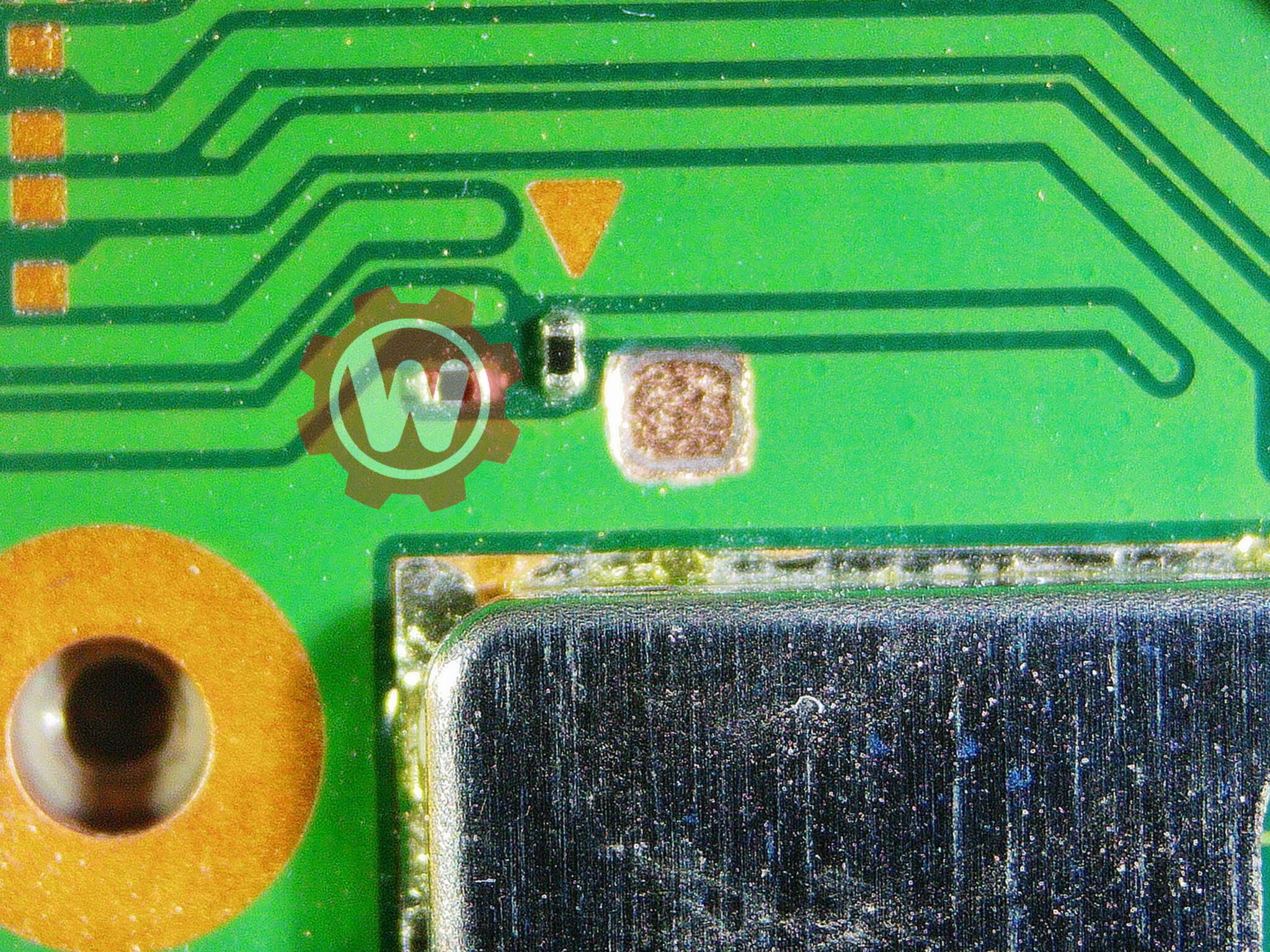
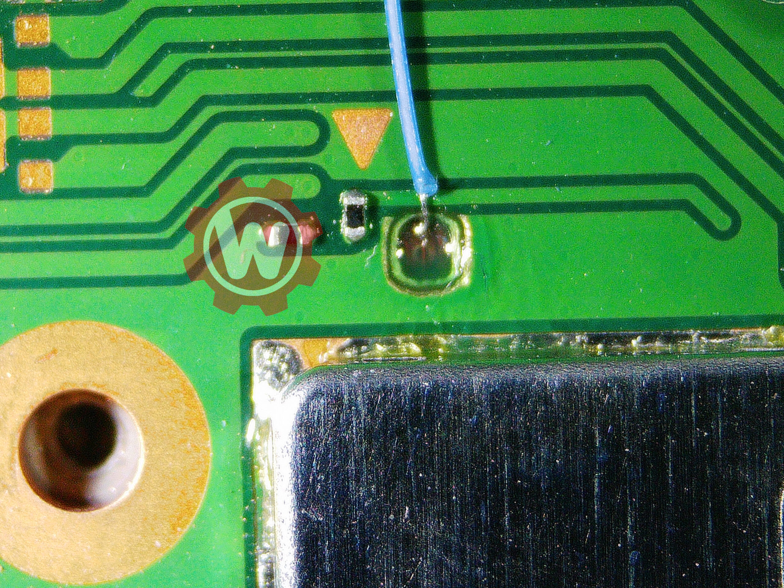
Marginal solder joints — usually the DAT0 trace connection is weak. Add more solder or rework the wire. |
| Black screen / no response | SoC ribbon cable misaligned or SP1/SP2 joints bridged to adjacent caps |
| Intermittent or unreliable boot | Loose magnet wire on the DAT0 trace, or marginal CMD resistor joint |
| CMD-related error | CMD resistor partially lifted from the board or cold joint on the A point |
| DAT0 trace diode reading out of range | Wrong trace exposed, or trace damaged during grinding. Verify location 1mm from A point. |
Wrapping Up
The Kamikaze method is the most permanent and reliable DAT0 connection method available on the OLED, but it carries the highest risk of any modchip installation procedure. The margin for error during grinding is genuinely a fraction of a millimeter — if you’re not comfortable with that level of precision work, the DAT0 adapter method achieves the same end result with much less risk.
If you do go forward, take your time, keep the area wet during grinding, verify the trace before soldering, and don’t skip the test boot in Step 05. For detailed error code lookup, see the NH-Switch Modchip Installation Guide troubleshooting page.
Credit for the Kamikaze method development goes to Stashboy and DefenderOfHyrule.
Need Professional OLED Kamikaze Installation?
We offer professional Nintendo Switch OLED Picofly modchip installation using the Kamikaze method, with expert microsoldering and post-install testing.
View Installation Services